Advanced PCB Protection
- Electronics packaging often becomes a bracket and fastener problem. We integrate packaging features into molded carriers to simplify builds.
- Potting workflows can slow iteration and complicate rework. We enable protective coverage approaches that reduce dependence on slow, multi-step potting.
- Conventional molding conditions can constrain molding directly onto electronics. We enable mold-around-electronics concepts that expand design options while reducing the need for multi-step potting workflows.
Connectors
- Instead of multi-part retention schemes, we integrate retention and alignment into molded connector structures to simplify assembly.
Film Overlays
- Post-applied overlays add labor and wear points. We integrate films into molded surfaces for durable UI and branding with fewer secondary steps.
Enclosures & Housings
- Prototype-to-production is often constrained by enclosure manufacturing. We support a clear path to scalable molded housings once designs are ready.
- Precision sensor builds can be limited by tolerance stack-up. We enable molded housings with integrated datum features to reduce adjustment effort.
- High-shear processing can restrict reinforced options. We enable more workable reinforced polymer choices for molded mounts and brackets.
Optical Components
- Optical programs often stall on stress-driven variability. We enable molding approaches that support more consistent optical-grade parts and carriers.
Thermal Management
- Many thermal solutions add interfaces and assembly steps. We enable molded thermal structures that support more integrated thermal pathways using filled polymers.
- Thermal interface stacks are often assembly-driven. We enable molded thermal interface structures that reduce interfaces and support filled polymer use.
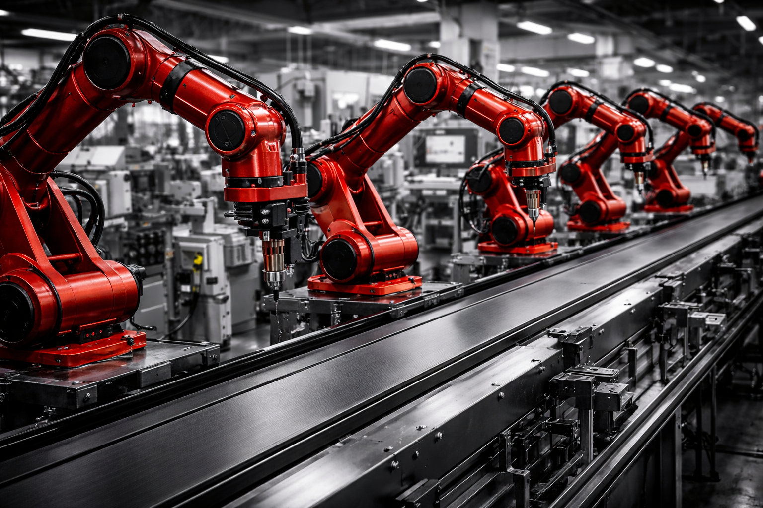
Manufacturing for High Tech Products and Systems
High tech products often face thermal constraints as power density increases in compact electronics, optical modules, and compute-adjacent hardware. Traditional approaches rely on metal heatsinks, gap pads, adhesives, and stacked thermal interfaces, which add assembly steps, tolerance sensitivity, and performance variability. At the same time, high-shear molding, conventional overmolding, and potting introduce warp, fiber damage, bonding inconsistency, and internal stress—driving designs toward bracketed assemblies and secondary operations to protect electronics, optics, and thermal paths as production scales.
Controlled injection molding, overmolding, insert molding, and low-stress encapsulation enable thermal and mechanical functions to be integrated more directly into molded structures. Thermally filled polymer systems (including ceramic- or graphite-based fillers) can be processed with more consistent dispersion and reduced anisotropy, supporting predictable heat transfer without the interface stacking typical of metal-plus-pad architectures. This allows heatsinks, thermal interface features, and electronics carriers to be combined into fewer molded parts while maintaining dimensional stability and repeatable contact geometry. For enclosures, sensor housings, precision optics, and high-power electronics, reduced internal stress improves optical alignment, bonding reliability, and thermal consistency at volume. The result is simpler assemblies with fewer interfaces, improved thermal repeatability, and manufacturing processes better aligned with the precision and scalability demands of high tech manufacturing.